Header image  

Nanoelectronics Group

 
line decor
  
line decor


  InN  


Nanowire Electro-optic Devices
To properly implement single nanowire devices, one is required to understand its working mechanism, which is not always as trivial as is often assumed. This was recently shown in the case of single nanowire light emitting diodes.

In a collaborative study with the groups of Professor Federico Capasso and Professor Venky Narayanamurti at Harvard |University, it was shown that the commonly assumed p-n junction between mechanically contacted wire-substrate or wire-wire devices is fairly unlikely, while the carrier transport across the junction is in most cases by tunnel injection.

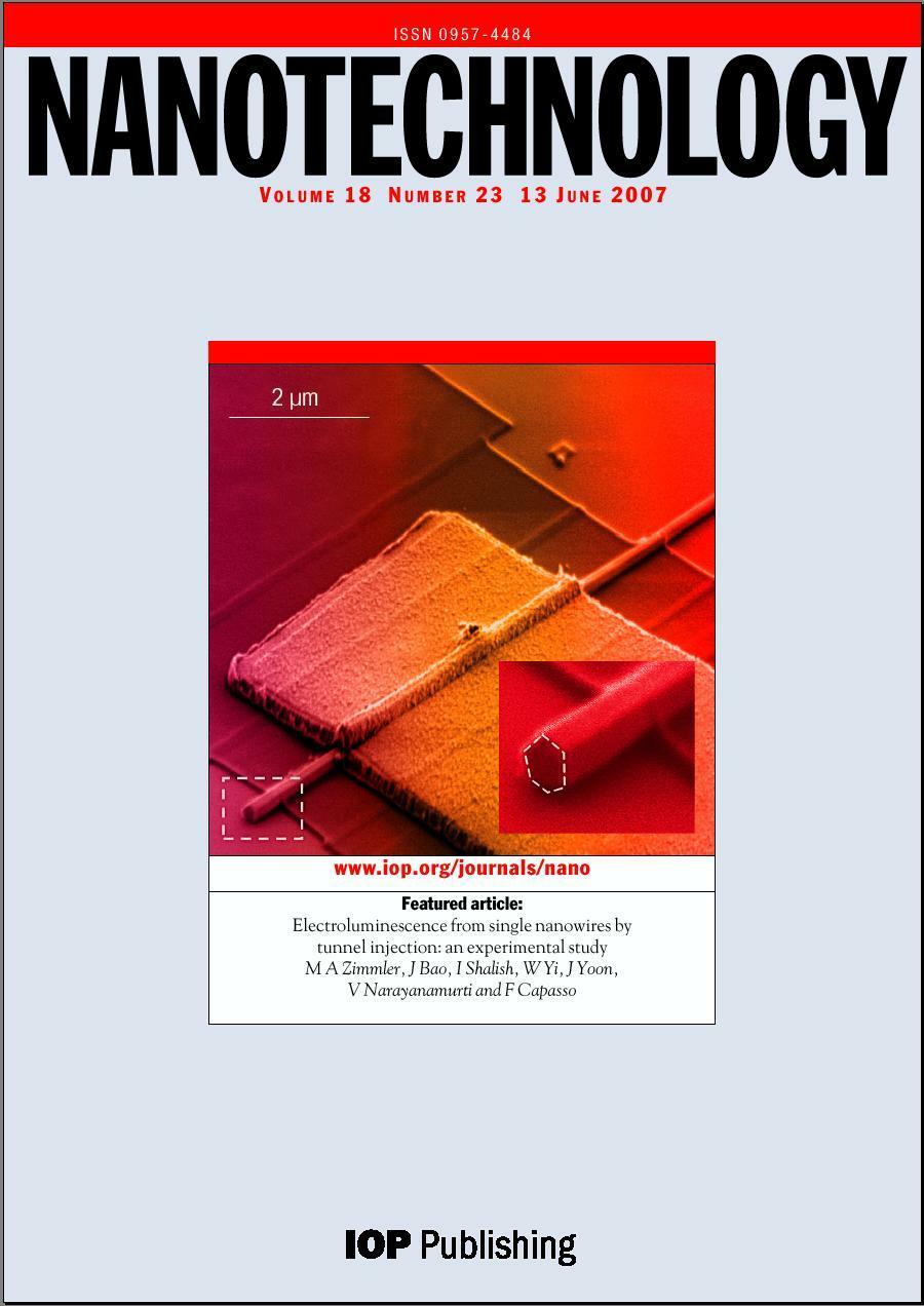
This was recently reported as a cover story in Nanotechnology (see paper)
and highlighted in Nanotechweb.org

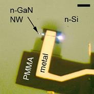
One of the surprising consequences of the tunnel junction is the finding that light emission also results when the n-type nanowire (GaN) is placed on an n-type substrate (Si). A novel feature of this unipolar device is that by reversing the polarity of the applied voltage the luminescence can be selectively obtained from either the nanowire or the substrate, i.e., a two-color unipolar LED.

This work was recently reported as a featured article in Nanotechnology (see paper) and highlighted in Nanotechweb.org and Optics.org