|
 |

| Nanowire Electronic Devices |
Understanding certain nanowire properties requires the preparation of a single nanowire device. For example, it is currently not feasible to use Hall effect to measure carrier mobility in nanowire, and therefore the only way is to create a field effect transistor and measure field-effect mobility.
To properly implement single nanowire devices, one is required to understand its working mechanism, which is not always as trivial as is often assumed. |
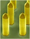
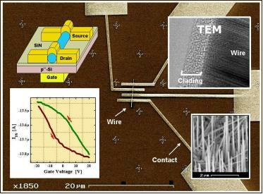
The image shows a single nanowire field effect transistor, which structure is illustrated in the top-right inset. The as-grown wires are shown at the bottom-left inset. The top-left inset shows a TEM of the wire surface, and the bottom-right inset is a current-voltage characteristic showing a memory effect caused by the cladding.
|
|
|
|
|