OLED research
OFET research
Organic Solar Cells (OSC)
Solar energy is the current leading venue for alternative green energy. However, the commercial solar panel holds some major disadvantages such as:
On the other hand, Organic Solar Cells (OSC) are promising candidates as a new way to utilize solar energy. The OSC can be installed in a variety of urban places such as buildings and shades as well as in transportation, clothing and autonomic devices. It is due to their unique properties such as mechanical flexibility, lightweight, and transparency.
All these properties can combine to a low-cost large-area device with an undemanding fabrication process. Their huge advantage is the variety of organic semiconducting materials and the ability to engineer new ones with improved qualities. Nowadays, the efficiency record was reached 14%.
1. A new model of organic solar cells reveals open circuit conditions and size-dependent power loss induced by the finite conductivity of a transparent contact
Link to paper: https://aip.scitation.org/doi/abs/10.1063/1.4974537
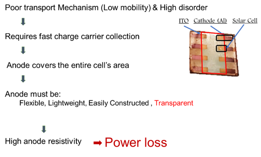
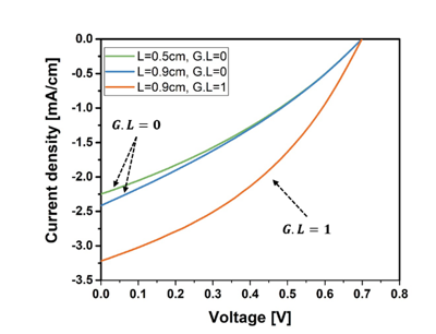
Organic Solar Cells (OSC) performance is highly size depended. Experiments show that by increasing the area of the device, its efficiency is rapidly decreasing. The observed losses are attributed to the transparent anode. Due to a very short charge carrier lifetime in organic materials, it requires a fast charge carrier collection. This compels the electrodes to overlay the entire organic layer, thus the polaron (the charge carriers within the organic material) will flow perpendicular to the contact in the shortest trajectory. Therefore, at least one electrode must be transparent. The downside of transparent materials (i.e. Indium-Tin-Oxide or ITO) is their low conductivity which reduces the output power of the cell and the power loss increases as the device getting larger. Hence, efficiencies higher than 10% has been achieved only for small-scale devices in which the size of the electrode was negligible.
In this research, we have developed a new approach for modeling the size dependence of the OSC efficiency. The model links together the two main layers affecting the size dependency of the device, i.e. the organic active area and the transparent electrode. The organic active area is based on the drift-diffusion model together with the Onsager-Braun theory while the transparent electrode is described by the Laplace equation. The link between the two sub-domains is done by an iterative process that matches the boundary conditions along their mutual interface. Our results revealed that as the cell increases, the regions far from the contact exhibit near open-circuit conditions which, in consequence, do not contribute to the output current.
2. Metal-Grid Modeling and Optimizations for Organic Solar Cells
To overcome the issue of the size dependency of organic solar cell (OSC) efficiency there is a need for implementing metal-grid on top of the transparent electrode. It transforms the large OSC into a module of several smaller cells. However, it introduces many other difficulties. It impairs the flexibility of the cell, it reduces the transparency which reduces the input light intensity and makes it difficult to be used in applications such as smart windows, and it requires additional processing which complicates fabrication and raises additional costs. A resulting benefit is the ability to create different textures, patterns, and designs for different purposes. It raises the need for an optimization tool to examine the trade-off between cell performance and the coverage of the metal grid.
In the previous work, we have developed a device modeling which takes into consideration the various parts of the device, namely, the organic active layer, both electrodes, and the interactions at the different interfaces. In this work, we have expanded the model to include the key element, the metal-grid. In the simulation, we can control the number, the size, and the position of the grid lines in the cell. Therefore, the simulation can aid in performing grid shape optimizations already at the early stages of the design of the OSC. This simulation has revealed several important guidelines for the design of the metal grid, including its positioning and its shape.
3. The role of the dielectric nature of the transparent contact in charge injection and collection in organic optoelectronic devices
Link to paper: https://journals.aps.org/prapplied/abstract/10.1103/PhysRevApplied.12.014029
In organic optoelectronics, the contacts are made from conductive transparent materials such as the degenerate semiconductor Indium-Tin-Oxide (ITO), the polymer PEDOT:PSS or graphene which are all dielectrics. In this work, we study the influence of the dielectric properties of the contact on the organic optoelectronic device performance. Many studies dealing with the dielectric properties from the optical point of view, e.g., absorption, transmission, and reflection. However, the electrical aspects of the device the dielectric properties of the contact are not manifested in the various models. Our aim is to pinpoint the importance of the dielectric property of the contact to the process of current injection and collection into and from the device.
To show that, we performed an electrical simulation using the Scott-Malliaras boundary conditions which describe the current flow of charge carriers into and from the organic layer. Their original model considered the effect of image-potential which reduces the injection barrier at the contact/organic interface, however, they only regarded for a metal contacts case. In this work, we have modified their model and added the correction for the case of dielectric contacts. Our results revealed that the current density of the device with a dielectric contact has been reduced by more than half with respect to a device with a metal contact. Moreover, we showed that similar results can be obtained with reduced mobility. It might explain why this issue was not mentioned before, it is since satisfactory fitting to experimental results could be obtained also without this parameter. However, this highlights the importance of using correct physics. We believe that our correction is very important and must be considered in future simulations. Hopefully, it will be a standard in commercial organic semiconductor simulation software and will aid in the future design of transparent contacts.
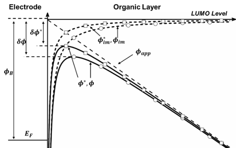
Due to the image-potential effect, the injection barrier reduces. Thus, the injection current increases. It is seen that for the dielectric contact, the barrier is lowered by a smaller amount resulting in lower currents.
Organic Light Emitting Diodes (OLED)
1. Microscopic investigation of degradation processes in a polyfluorene blend by near-field scanning optical microscopy
Link to paper: https://doi.org/10.1021/acs.macromol.6b01543
The paper describes a new approach for the study of degradation processes and stability dependence on a sub-micron length-scale in a polyfluorene blend as a function of blend and phase composition using time-dependence near-field scanning optical microscopy (NSOM).
Usually the degradation is characterized by macroscopic quantities such as electrical current and optical properties using far-field techniques. Using NSOM, we performed high-resolution spatial distribution mapping of the PL and its time evolution, which enabled degradation study on a microscopic, micron and sub-micron scale. By mapping the local PL emission over time we show that the contrast of the NSOM changed with time due to different degradation rates, and was determined by the ratio between the emission from the higher-lying, F8BT-rich phase and the lower-lying, PFO-rich phase. We show that while the degradation of F8BT was driven by photo-bleaching and the absorption remained almost unchanged, both faster absorption degradation and photo-bleaching processes dominate the degradation of PFO. Hence the efficiency of the energy transfer from the PFO to the F8BT is hampered resulting in the observed contrast change. In addition, we demonstrated that energy transfer does not protect the PFO from degradation and does not improve its resistance to oxidation.
Figure 1: PL mapping using NSOM
A phase-separated film allowed us to thoroughly examine the degradation process on a sub-micron length-scale by local PL mapping using near-field scanning optical microscopy
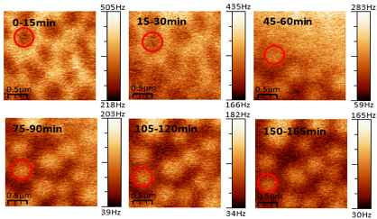
Figure 2: PL temporal evolution
The contrast of the NSOM image changed with time, from stronger emission of the PFO-rich phase to higher emission of the F8BT-rich phase.
2. The role of electron injection efficiency in determining the transient electroluminescence in organic light emitting diodes
The paper describes a unique approach for the study of the transient electroluminescence (TREL) dependency of an OLED on the cathode’s electron injection efficiency, after driving the OLED to an open-circuit condition.
The new proposed approach differ from what is previously reported in the literature because it does not drive the OLED to an off-state by driving it to short-circuit condition neither using high reverse currents to discharge the free carriers as in commercial drivers. Both approaches affect the distribution of charges within the device during switching. In contrast, our self-developed driver can facilitate a switching time of ~5ns that maintains the steady-state charge distribution within the device, with minimal effect on the distribution of the charges during the switching. As we show in the paper, there is a distinct difference between the measured TREL of the OLED after switching off the voltage using our technique and common available techniques. Using our approach, we studied the dependence of the TREL on the electron injection efficiency. The transient EL reveals a behavior of two exponential decays, both with a lifetime much longer than the exciton’s life-time measured via time-resolved photoluminescence. We found that the electron injection efficiency has a significant effect on the slow EL decay and that enhancing the injection efficiency leads to a longer EL decay. A physical explanation supported by a device simulation based on the Drift-Diffusion model suggests that the EL originates from the radiative recombination of newly formed singlet excitons formed by the discharge of the space charge regions under a nearly constant electric field. The longer decay time resulted from a higher voltage-drop on the space charge regions when the injection efficiency is higher.
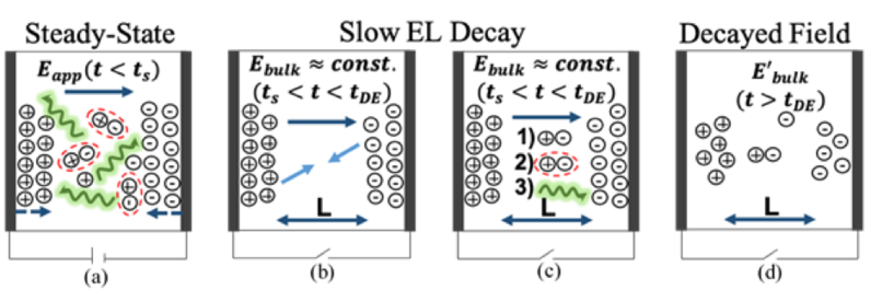
a) Light emission under steady-state condition. b) After driving the OLED to an open-circuit condition, the developed voltage does not immediately change and stays constant even without an applied voltage. c) A discharging of the space charge regions via a drift of charges, excitons formation, and radiative recombination under a constant electric field. d) The electric field is decayed and the system cannot be represented by a constant lifetime any longer. Notation: ts - switching time, tDE - a decayed electric field time, Eapp - an applied electric field, Ebulk - a constant electric field in the area out of the space-charge regions, Ebulk' - a decayed electric field in the area out of the space-charge regions, L - bulk thickness.